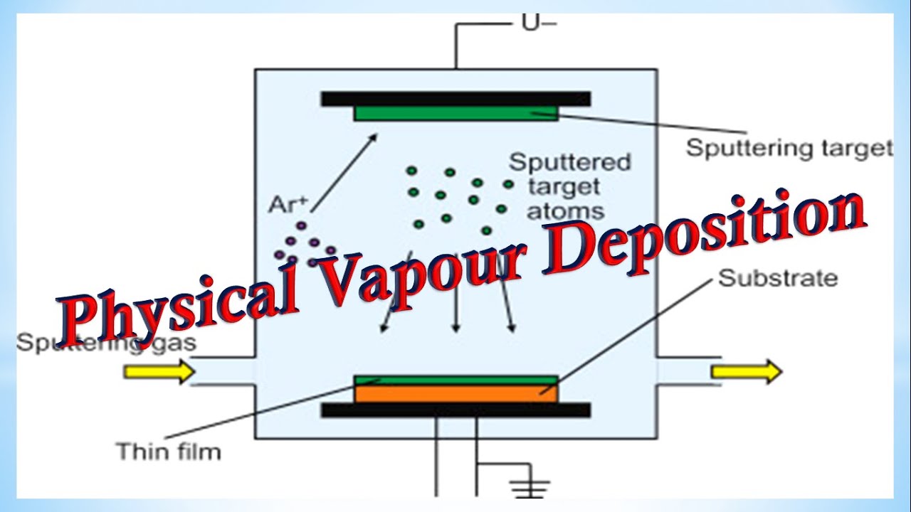
A schematic illustration of physical vapor deposition (pvd) process for Principle of chemical vapor deposition (cvd) The schematic diagram of chemical vapor deposition system.
(a) Conceptual diagram of the chemical vapor deposition process in
Atmospheric pressure chemical vapor deposition of graphene
Chemical vapour deposition (cvd)
Deposition vapor schematicSchematic diagram of the chemical vapor deposition method. What is chemical vapor deposition (cvd)?What is chemical vapor deposition (cvd)?.
Cvd deposition vapor mos2 synthesis nanoparticles sio2 epitaxial substrate mose2 atomic layers tmdDeposition vapour Deposition vaporDeposition vapor schematic beam electron directed plume airfoil evaporated.

What is chemical vapor deposition (cvd)?
Deposition cvd vapor method principleExplained: chemical vapor deposition Cvd pecvd deposition chemical vapour 2d chamber plasma tools process diagram system 1d processes oxford electrode nanomaterials technology gas cleaningWhat is chemical vapor deposition (cvd)?.
(a) schematic of chemical vapor deposition technique demonstrating theSchematic diagram of the used horizontal chemical vapor deposition Schematic of physical vapor deposition for tio2 coatingDeposition vapor schematic flakes ultrathin photodetectors structural.

Dr. hicks' lab
Deposition cvd chemical vapor process explained coating mit nanotechnology material carbon coatings pressure nanomaterials technology power properties uniform polymer metalsDeposition vapor tio2 coating (a) conceptual diagram of the chemical vapor deposition process inVapor deposition conceptual cuo grew.
Pressure chemical deposition graphene atmospheric vapor intechopen figureSchematic diagram of the chemical vapor deposition method. b Deposition chemical vapor mocvd surface uclaDeposition chemical vapour setup.

7 schematic illustration of physical vapor deposition (pvd) process
Deposition vapor cvd representationDeposition vapor chemical electron transmission (a) schematic of the chemical vapor deposition equipment; (bSchematic diagram of the used horizontal chemical vapor deposition.
(a) schematic of chemical vapor deposition setup. (b) schematicSchematic of a basic plasma enhanced chemical vapor deposition system Schematic diagram of the chemical vapor deposition apparatus employed| the schematic of initiated chemical vapor deposition reactor.

Schematic diagram of chemical vapor deposition setup
Schematic diagram of chemical vapour deposition setup.Schematic diagram of (a) the initiated chemical vapor deposition and (color online) schematic illustration of a directed vapor depositionSchematic diagram of chemical vapor deposition setup.
Chemical vapor deposition (cvd) method: (a) schematic illustration of3 a schematic representation of the chemical vapor deposition (cvd Deposition vapor schematic fig contextVacuum deposition.

Physical vapour deposition
Vapor deposition schematic demonstrating components pecvd microwave reprinted .
.